1. Computational Metrology for Nanostructures: Problems and Solution Methods

In order to achieve effective process control, fast, inexpensive, nondestructive, and reliable nanometer scale feature measurements are extremely useful in nanomanufacturing. Optics-based metrology tools, which have drawn more and more attention in semiconductor manufacturing because of their attractive advantages, such as low cost, non-contact, non-destruction, and high throughput, may be one of the best choices. Overall, optics-based metrology can be classified into two categories, namely the model-free and the model-based methods. Model-free metrology, such as the conventiona...[more]
2. Optical Ellipsometric Scatterometry: Instrumentation and Applications
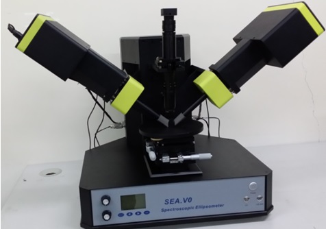
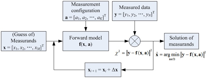
Optical ellipsometric scatterometry techniques, such as scatterometry based on conventional spectroscopic ellipsometry (SE), have currently become one of the most important approaches for in-line metrology of geometric parameters and nanostructures in high-volume-production nanomanufacturing, due to their attractive advantages of high throughput, low cost, non-contact, and non-destruction. Optical ellipsometric scatterometry is essentially model-based metrology, which involves two key issues - how to collect highly precise ellipsometric scattering data, and how to rapidly and accura...[more]
3. Computational Lithography: Forward Optical Imaging Simulation and Inverse Source Mask Optimizatio...
193nm ArF immersion lithography is widely used in the semiconductor industry to manufacture integrated circuits whose critical dimensions are much smaller than the source wavelength. The manufacturing process is similar to creating thin lines with a broad brush, which is physically beyond the resolution limit. Computational lithography (CL) enables this process and guarantees high volume production as well. It has been a driving force of Moore's Law. Computational lithography models the lithography process, including the imaging system (illumination source, mask, and projection lens...[more]
4. In-Situ Aberration Measurement in Optical Lithography: Fast Imaging Modeling and Aberration Retri...
With ever decreasing feature sizes, the impact of lens aberration has become increasingly important for imaging quality control of projection lithographic tools. The imaging optics configuration in lithographic tools is typically a partially coherent system characterized by the intensity distribution of the source and the pupil function of the projection lens. Imaging properties of such partially coherent systems have to be described using a bilinear model, which leads to time-consuming calculations and difficulties in comprehension, especially in the case when wavefront aberration ...[more]
5. Model-Based Infrared Reflectrometry for Micro/Nano Deep Trench Structures
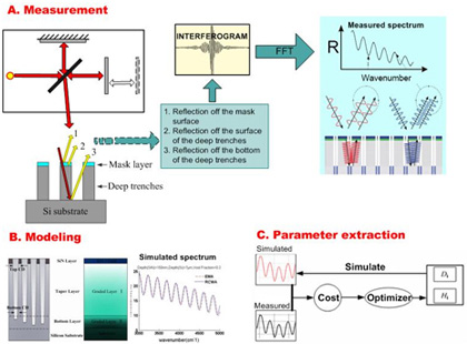
Deep trench structures with high aspect-ratio have been widely used in microelectronics such as capacitors in advanced dynamic random access memory (DRAM) devices. As deep trench devices have been packed more tightly, the critical dimension (CD) and depth dependent features must now be monitored to ensure process control. Model-based infrared reflectrometry (MBIR) is an optical metrology that has been introduced recently for measuring high aspect-ratio periodic trench structures. The trench structure is modeled as a multilayer thin film stack with effective medium approx...[more]
6. Optical Method and System for MEMS Dynamics Characterization
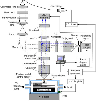
Measurement and testing of microstructure dynamics is necessary to develop reliable and marketable microelectromechanical system (MEMS) products. However, it is not easy to test MEMS dynamic behavior because of its micro structure, high frequency response upon excitation and complex operation environment. We have investigated the optical methods potentially suitable for MEMS dynamics characterization, and developed a measurement system for surface topography, three-dimensional motions, and modal parameters of MEMS.[more]